
In my latest blog article Surface analysis techniques for medical technology devices, I told you that we recently invested heavily in advanced surface analysis equipment. In this article I am getting a bit more into the details about what we actually can measure with our new equipment.
A scanning electron microscope for advanced analytical applications
Our new Scanning Electron Microscope (SEM) is equipped with various features. It can produce high-resolution images of surface structures, and has a very high magnification range of up to 60,000X. It can perform relative quantification of a material’s elemental composition and is also able to image polymer surfaces.
Information on material composition and topography
The microscope is equipped with two types of electron detectors; one that detects backscattered electrons (BEI) and one that detects secondary electrons (SEI). Common to both of these modes of detection is that the resulting image is generated from the intensity of the signal reaching the detector. The grayscale image represents the electron count of the detector resulting from a specific position of the electron beam on the sample surface. As a result, dark areas represent a relatively lower electron count compared to brighter areas.
Using the BEI detector, the resulting image contains a high degree of information on the material composition as more electrons are backscattered from heavier atoms at the surface compared to the amount reflected from lighter elements. The SEI detector provides images with a high degree of topographical information. This is a result of the depth, within the samples, at which these electrons are emitted. Also, the SEI detector is better suited for obtaining high quality images at larger magnification.
Low vacuum mode enables imaging of polymers
Due to the nature of the electron microscope, high quality images require good electrical conductance of the material being examined. This can cause some difficulties when imaging for example polymeric materials as negative charge, building up on the surface of the material, will deflect the incoming electrons used for imaging. For such materials the microscope is equipped with a low vacuum mode. Running the microscope in this mode introduces charge carriers in the form molecules from the ambient air. This reduces the degree of sample charging and enables the imaging of poorly conducting materials, such as polymers.
Using the SEM for determining chemical composition
Elemental analysis, using the SEM, is based on the detection of characteristic X-rays. These are generated by the interactions between the incident electrons, and the electrons of the atoms comprising the sample. The majority of the collision events, that generate such X-rays, take place below the surface of the material. As a result, the probing depth of the Energy Dispersive X-Ray Spectroscopy System (EDX) is typically a few micrometres. One of the factors affecting the probing depth is the acceleration voltage used for the analysis.
The analysis is performed by scanning the electron beam over the area of interest, while collecting the complete X-ray spectrum. From the collected spectrum, the chemical composition can be calculated. The method is semi-quantitative, as the elemental composition is expressed as a function of the total number of elements included in the analysis. When generating characteristic X-rays, the acceleration voltage of the incoming electrons, is highly important. Some elements can be detected using a relatively low acceleration voltage, while detection of others requires a higher voltage.
Our new microscope is capable of operating with three different acceleration voltages. This enables detection of a wide range of elements, including carbon, titanium, vanadium, aluminium, chromium, cobalt and tungsten. As a result, the EDX system can e.g. be used for distinguishing between grade 4 and grade 5 titanium. Another option with the EDX system is to perform elemental mapping of surface features, resulting in an overview of the spatial location of elements.
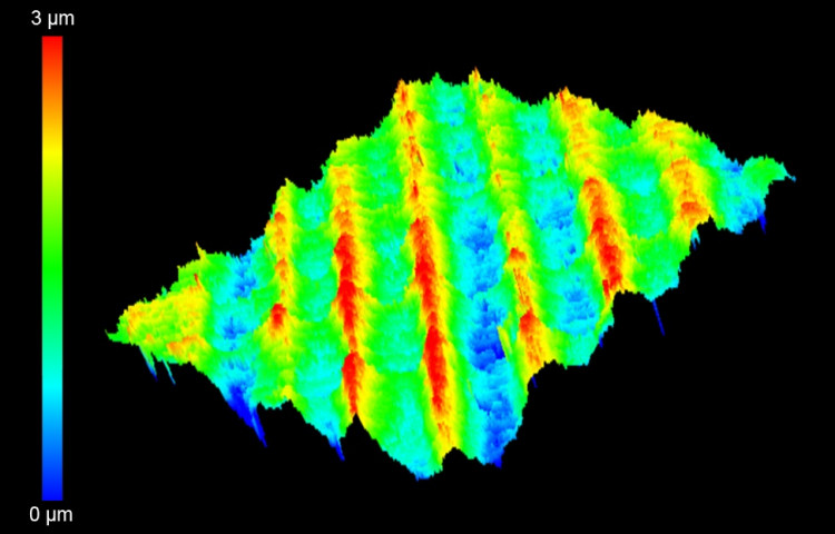
Specialised optical microscope enables measurement of surface roughness parameters
Our white light interference surface profiler is a specialised optical microscope that uses optical interference to detect the focal point on the surface of a sample. Using piezoelectronics the height position of the microscope lens can be varied with a high degree of precision, in steps of around 10 nanometres. By continuously varying the height position of the lens, while detecting the interference pattern resulting from the surface, the focal point can be determined for each position of the area being imaged. This results in a 3D topographical map of the surface. Via the equipment software, the acquired data can be treated to allow for calculating both classical 2D surface roughness parameters as well as 3D parameters.
The size of the analysed area depends on the objective lens used for the analysis. The lens also determines the resolution of the acquired 3D data set. Larger surface roughness values can be determined using an objective lens with low magnification. Lower surface roughness values require an objective lens with a higher magnification.
X-Ray fluorescence for fast and reliable identification of materials
While our SEM/EDX system is capable of determining material compositions, this approach is relatively time consuming and sets certain limits to the size of the sample being analysed. Our new X-Ray Fluorescence analyser (XRF) is also capable of determining the elemental composition of metals but does this under ambient conditions and is, furthermore, not limited by the size of the sample being analysed. The XRF analyser utilizes the principle of X-ray fluorescence. When radiating a sample with X-rays, the sample atoms will generate characteristic X-ray emission. Similar to the EDX analysis of the SEM, the emission can be used qualitatively to both determine and quantify the elements of the material. The penetration depth of the incident X-rays is significantly larger than for the electrons used by the SEM/EDX. As a result, the XRF analysis determines the bulk composition of the material and is, thus, better suited for e.g. verifying that the correct material is being used for the production of a specific part.
Every aspect of our manufacturing process, from design to distribution, must meet strict quality standards. Not only our customers, but also vendors, suppliers, contractors, OEMs and third parties need to be sure that their products comply with medical device rules and regulations. With our new surface and material analysis equipment, we can find and minimise possible risks in the manufacturing process. We can improve and refine processes, contributing to our state-of-the-art production facilities, and ensure that we meet these strict quality standards. Having this equipment in-house, we can measure more often and with greater accuracy than before. It provides a higher product quality, and minimises the risk that a product that doesn’t meet the quality standards, is delivered to the customer.
Did you find this article interesting? Let me know by sharing it on LinkedIn! There you can find more updates and news from the medtech industry and Elos Medtech. Also read Surface analysis techniques for medical technology devices.


